In the process of converting Solar Light into Electricity, one of the major components used is the Solar Panel. These are the devices which absorb sunlight and thus facilitating any further process. Any cell which is able to convert Sunlight into Electricity is often termed as the Photovoltaic Cell. These types of cells are made with semiconducting materials such as Germanium or Silicon so that they can withstand heat.
Construction of the cells
Normally, most of the current day solar panels are made with Silicon. Then based on the arrangement of these silicon cells, the solar panels can be further divided into two types - Amorphous and Crystalline.
Crystalline Solar Panels are those in which the Photovoltaic cells are arranged in repetitive units while Amorphous Panels are those in which the cells are arranged in a randomized manner. Usually, the efficiency is more in crystalline cells as they have repeating structure but the amorphous ones are cheaper as you don’t have to spend much time and effort in arranging the crystals.
At present, the most renowned and effective Solar Panels are the Crystalline Silicon ones. In these types, a rather pure form of silicon along with high quality crystals has to be used in order to produce maximum efficiency. The structure of Silicon is complex. On the outer surface, it has four electrons and in order to obtain a stable gas configuration, it has to form two bonds with neighboring atoms which it does.
Now, when light or heat is applied externally over this configuration, it will break it. So, when sunlight is incident over the Silicon Crystalline solar panel, it will break the stable configuration of the panel resulting in the formation f electron vacancies.
Crystalline Silicon Solar Cell Technology
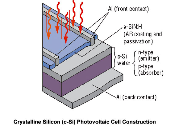
Conductivity of the cells
The presence of these vacancies give rise to a condition called as Intrinsic Conductivity. It becomes impossible for the electron to conduct electricity in such a condition. So, the vacancy produced in the structure has to be satisfied by mixing it with a suitable material like Boron or Phosphorous which has the structure to satisfy such a condition. If phosphorous is added, the doping (mixing impurities in order to make the material conductive) process is called as n-doping on the other hand, if Boron is added, the process is called as p-doping.
The n-doping is more effective than the p-doping. In n-doping, the electron will be allowed to move freely thus creating the ability to transfer charges. But in the p-doping, the vacancy filled will be regenerated in a new place causing further intrinsic conduction.
If both the p area and the n area are brought together, the structure will be known as the p-n junction, this junction facilitates the movement of n-ions to the positive and p-ions to the negative region forming an electric field in the process. This electric field can be withdrawn and it can be used to power out houses. So, technically this p-n junction is called as the Solar Cell in this case. This junction is arranged repetitively on your rooftops in order to absorb sunlight.